I/O & Pinout
Connector Diagram
SuperSeal Connector Diagram -- Looking into the connector
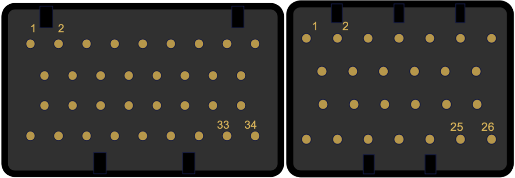
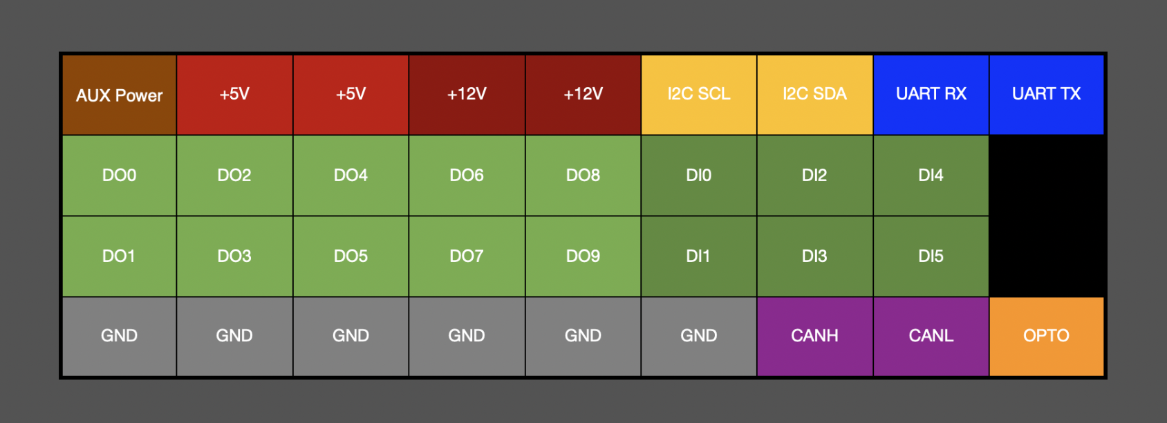
34-Pin Connector Pinout
|
Pin Number |
Pin Name |
Description |
| 1 | AUX Power |
12-32VDC power supply input. Hot-swappable with PoE. |
| 2 |
+5V |
5VDC, 1A output supply |
| 3 |
+5V |
5VDC, 1A output supply |
| 4 |
+12V |
12VDC output supply. 2.5A if using AUX, 1.4A if using PoE |
| 5 |
+12V |
12VDC output supply. 2.5A if using AUX, 1.4A if using PoE |
| 6 | SCL | I2C Bus SCL |
| 7 | SDA | I2C Bus SDA |
| 8 | UART RX | This is not crossed-over on our side. Connect to another device’s TX pin. |
| 9 | UART TX | This is not crossed-over on our side. Connect to another device’s RX pin. |
| 10 | DO0 | 0-3V3 sourcing digital-outputs. NOT ISOLATED, DUT must be grounded to DAQAstra. PWM on TIMER 11 |
| 11 | DO2 | PWM on TIMER 4 |
| 12 | DO4 | PWM on TIMER 8 |
| 13 | DO6 | PWM on TIMER 9 |
| 14 | DO8 | PWM on TIMER 2 |
| 15 | DI0 |
Digital-Inputs are isolated. Use the jumpers on DAQAstra to use the internal 5V as the open-drain input's logic-high. Use the OPTO selection to use an external voltage, instead. All digital-inputs share the same logic supply. Add series resistors to current-limit. 500 ohm for 12V, 1000 ohm for 24V. |
| 16 | DI2 | |
| 17 | DI4 | |
| 18 | DO1 | PWM on TIMER 10 |
| 19 | DO3 | PWM on TIMER 4 |
| 20 | DO5 | PWM on TIMER 9 |
| 21 | DO7 | PWM on TIMER 3 |
| 22 | DO9 | PWM on TIMER 2 |
| 23 | DI1 | |
| 24 | DI3 | |
| 25 | DI5 | |
| 26 | GND | Ground |
| 27 | GND | Ground |
| 28 | GND | Ground |
| 29 | GND | Ground |
| 30 | GND | Ground |
| 31 | GND | Ground |
| 32 | CANH | |
| 33 | CANL | |
| 34 | OPTO | External supply for DI pins |
26-Pin Connector Pinout
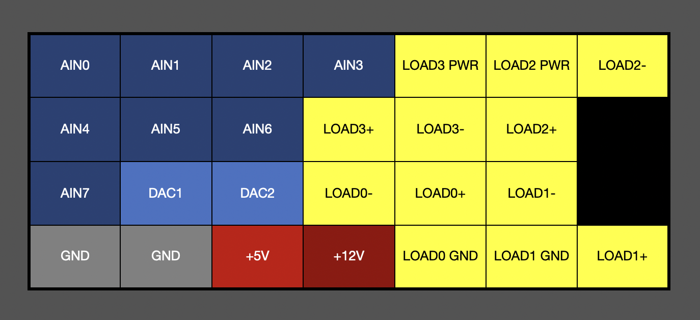
|
Pin Number |
Pin Name |
Description |
Notes |
| 1 | AIN0 | Analog-to-Digital Converter Input 0 | 0 - 5V, 12-bit. Input buffered using voltage-follower. |
| 2 | AIN1 | Analog-to-Digital Converter Input 1 | 0 - 5V, 12-bit. Input buffered using voltage-follower. |
| 3 | AIN2 | Analog-to-Digital Converter Input 2 | 0 - 5V, 12-bit. Input buffered using voltage-follower. |
| 4 | AIN3 | Analog-to-Digital Converter Input 3 | 0 - 5V, 12-bit. Input buffered using voltage-follower. |
| 5 | LOAD3 PWR | High-Side Solid-State Relay 3 Power Supply |
Connect the positive lead of voltage supply to power LOAD3. Must be <50V and external supply GND must be tied to a DAQAstra GND pin. |
| 6 | LOAD2 PWR | High-Side Solid-State Relay 3 Power Supply |
Connect the positive lead of voltage supply to power LOAD2. Must be <50V and external supply GND must be tied to a DAQAstra GND pin. |
| 7 | LOAD2- | High-Side Solid-State Relay 2 Load Cathode |
Switched load negative lead. Optional connection adding a flyback diode to clamp inductive spikes from switched inductive loads. |
| 8 | AIN4 | Analog-to-Digital Converter Input 4 | 0 - 5V, 12-bit. Input buffered using voltage-follower. |
| 9 | AIN5 | Analog-to-Digital Converter Input 5 | 0 - 5V, 12-bit. Input buffered using voltage-follower. |
| 10 | AIN6 | Analog-to-Digital Converter Input 6 | 0 - 5V, 12-bit. Input buffered using voltage-follower. |
| 11 | LOAD3+ | High-Side Solid-State Relay 3 Load Anode | Switched load positive lead. |
| 12 | LOAD3- | High-Side Solid-State Relay 3 Load Cathode |
Switched load negative lead. Optional connection adding a flyback diode to clamp inductive spikes from switched inductive loads. |
| 13 | LOAD2+ | High-Side Solid-State Relay 2 Load Anode | Switched load positive lead. |
| 14 | AIN7 | Analog-to-Digital Converter Input 7 | 0 - 5V, 12-bit. Input buffered using voltage-follower. |
| 15 | DAC1 | Digital-to-Analog Converter Output 1 | 0-5V or 0-12V, 12-bit analog output. The maximum output voltage is selectable via the DAC VCC jumper on the PCB. |
| 16 | DAC2 | Digital-to-Analog Converter Output 2 |
0-5V or 0-12V, 12-bit analog output. The maximum output voltage is selectable via the DAC VCC jumper on the PCB. The jumper controls both DAC channels. |
| 17 | LOAD0- | Low-Side Solid-State Relay 0 Load Cathode | Switched load negative lead. |
| 18 | LOAD0+ | Low-Side Solid-State Relay 0 Load Anode |
Switched load positive lead. Optional connection adding a flyback diode to clamp inductive spikes from switched inductive loads. |
| 19 | LOAD1- | Low-Side Solid-State Relay 1 Load Cathode | Switched load negative lead. |
| 20 | GND | GND | |
| 21 | GND | GND | |
| 22 |
+5V |
5V DC Output Power | 1.5A PTC Polyfuse in series with output. Voltage supply limited to continuous drain of 1A. |
| 23 |
+12V |
12V DC Output Power | This rail has OVP, UVLO, and OCP. Limited to 2.5A. |
| 24 | LOAD0 GND | Low-Side Solid-State Relay 0 Supply GND |
Connect the negative lead of voltage supply to power LOAD0. Must be <50V and external supply GND must also be tied to a DAQAstra GND pin. |
| 25 | LOAD1 GND | Low-Side Solid-State Relay 1 Supply GND |
Connect the negative lead of voltage supply to power LOAD1. Must be <50V and external supply GND must also be tied to a DAQAstra GND pin. |
| 26 | LOAD1+ | Low-Side Solid-State Relay 1 Load Anode |
Switched load positive lead. Optional connection adding a flyback diode to clamp inductive spikes from switched inductive loads. |
Pinout Legend
SuperSeal Pinout Legend
Power Outputs
- +5V**:** protected by a PTC resettable fuse rated at 1.5A. Generally used for power sensors or external modules.
- +12V: protected by a power-management integrated-circuit (PMIC), preventing current draw over 2.5A.
DAC - Digital-to-Analog Converter:
- Allows for the DAQAstra’s microcontroller to provide analog signals (e.g. a feedback control signal)
- The DAC can drive up to 60mA and features a low-pass filter with a 3dB cutoff at 160kHz.
- Outputs an analog voltage ranging from 0-12V with 12-bit/3 millivolt accuracy.
- The DAC is often used as a control-signal output for other controllers, like a mass-flow controller or DC-Motor drive. They are also often used in audio reproduction or as waveform generators.
AIN - Analog-to-Digital Converter:
- Allows for the DAQAstra’s microcontroller to read analog signals (e.g. transduced audio or temperature signals).
- All analog signals read through the SuperSeal are buffered by a unity-gain op-amp, providing stability in the measurement.
- Reads an analog voltage ranging from 0-5V with 12-bit accuracy, or 4096 1.2 millivolt steps across the measurement range.
- The firmware oversamples the 12-bit samples to achieve 16-bit data. This is often used for measuring analog information about the environment (temperature, humidity, pressure).
PLCIN - Isolated PLC Digital Input:
- Electrically isolated input, designed for -60–60V Discrete inputs, such as the 24V I/O often found on PLCs.
- Up to 4Mbps data rate
CAN Bus:
- Controller Area Network bus differential inputs (CAN_P and CAN_N), connected to a CAN Transceiver.
- Offers up to 1Mbps data rate.
DIO - Digital Input/Output:
- Sends or receives digital logic signals in 5VTTL. There are ten DIO pins, all capable of acting as either an input or output. All GPIO from the DAQAstra are protected via a level-shifter.
- NOTE: The level shifters that interface between the microcontroller and I/O pins do not drive the outputs to GND when the microcontroller pins are not driven (e.g. the board firmware is changing, or the board is disconnected). In this state, the outputs are High-Z (floating).
LOWSIDE - Solid-State Relay
- An array of four Gate Driver ICs, each connected to an N-Channel MOSFET. Acts by connecting/disconnecting a load’s current return to ground. Features a TVS diode in parallel with the MOSFET, allowing for overvoltage protection and safe connection of inductive loads.
- Rated for ~2A continuous current and up to 10A pulsed current.
- Users can choose between connecting the high side of their load to the board’s internal 12V output, or an external output. In the former case, GNDPWR and GND must be connected (as the Lowside switches use GNDPWR as their return). This is done by shorting the pins on the GND Isolation Jumper, shown in the board render above.
Auxiliary Power Input
- Auxiliary power enters from the 2-Terminal Female Input and is converted to Regulated 12V, via a switching converter. An Integrated Circuit switches between a supply voltage from PoE and the regulated 12V Auxiliary.
- The pin closest to the pin-one indicator is the VCC pin. The other is GND.